PCBWay has prospered as a global intelligent platform for electronic intelligent hardware by depending on its fundamental competitiveness of "on-time delivery capabilities" and "one-stop service."
First of all, among local PCB manufacturing firms, PCBWay has the fastest delivery capabilities. Single-layer and two-layer deliveries typically take 1-2 days, although they can be accelerated for 12 hours. The most recent lead time plan for Standard PCB orders of 1 to 5 square meters in small batches is 3 to 4 days, which is significantly quicker than the industry standard.
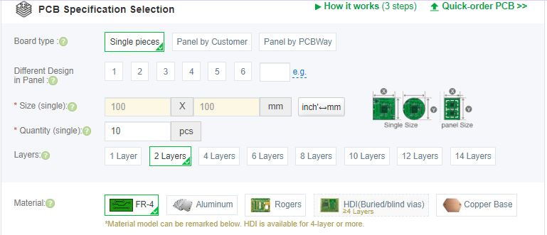
Second, PCBWay may provide clients a one-stop PCB manufacturing service, giving them access to a more affordable small-volume PCB business solution. Solutions design, signal integrity design, PCB front-end design, PCB manufacturing, PCBA assembly, testing, and more are all included in one-stop services. In addition to meeting client wants, this also entails enhancing the value of the business.
How To Choose a Basic PCB Material
Organic substrate materials and inorganic substrate materials are the two primary categories of printed circuit board substrates.
The majority of substrate materials are organic. For various layers, different PCB substrates are utilized. For instance, prefabricated composite materials are used in 3 to 4-layer boards, while glass-epoxy materials are primarily used in double-sided boards. The degree of bending of the printed circuit board during lead-free electronics assembly increases with temperature. As a result, plates with fewer degrees of bendings, such as FR-4 and other types of substrates, must be used in SMT.
Electrode peeling and decreased dependability will result from the substrate's effect on the element's stress during expansion and contraction. As a result, while choosing materials, extra attention should be paid to the material expansion coefficient when the element is bigger than 3.2 1.6mm. High copper foil adhesive strength (over 1.5 104Pa) and flexural strength (25 104Pa), high electrical conductivity and tiny dielectric constant, good punch ability (precision 0.02mm), and compatibility with cleaning chemicals are essential requirements for PCBs used in surface assembly technology. Additionally, there must be no warpage, cracks, scars, rust spots, or other defects, and the look must be level and smooth.
The printed circuit board measures 0.5mm, 0.7mm, 0.8mm, 1mm, 1.5mm, 1.6mm, (1.8mm), 2.7mm, (3mm), 3.2mm, 4.0mm, and 6.4mm thick, with 0.7mm and 1.5mm being the thickest. The twin-panel with gold fingers is designed using a PCB with a thickness of mm, and its non-standard sizes are 1.8mm and 3.0mm.
From a manufacturing standpoint, a printed circuit board's minimum single board size shouldn't be less than 250 x 200mm; often, the optimal size is (250 x 350mm) x (200 x 250mm). It is simple to utilize the puzzle method for PCBs with long sides less than 125mm or wide sides less than 100mm. A substrate with a thickness of 1.6 mm is specified by the surface assembly technique to bend with upper warpage of 0.5 mm and lower warpage of 1.2 mm. The typical acceptable bending rate is less than 0.065 percent.
The metal materials, it is separated into three categories as seen in ordinary PCBs. According to the soft and hard constructions, it is split into three categories. Similar to how standard PCB clone boards have evolved toward high pin counts, downsizing, SMD, and complexity, electronic plug-ins have as well. The pins used to attach the electronic plug to the circuit board are soldered on the opposite side. THT (ThroughHoleTechnology) plug-in technology is the name of this technology.
This is the standard PCB application. The demand for electrical connections on multi-layer circuit boards has arisen due to the quick growth of SMT chip technology. After drilling, which necessitates a variety of drilling equipment, electroplating is used to assure this. Different performance PCBs are now being launched both at home and abroad in order to satisfy the aforementioned standards.


